Äîêóìåíòàöèÿ è îïèñàíèÿ www.docs.chipfind.ru
REV. PrC
7/13/01
Preliminary Technical Data
PRELIMINARY TECHNICAL DATA
Information furnished by Analog Devices is believed to be accurate and
reliable. However, no responsibility is assumed by Analog Devices for its
use, nor for any infringements of patents or other rights of third parties
which may result from its use. No license is granted by implication or
otherwise under any patent or patent rights of Analog Devices.
=
AD7484
One Technology Way, P.O. Box 9106, Norwood, MA 02062-9106, U.S.A.
Tel: 781/329-4700
World Wide Web Site: http://www.analog.com
Fax: 781/326-8703
© Analog Devices, Inc., 2001
3MSPS,
14-Bit SAR ADC
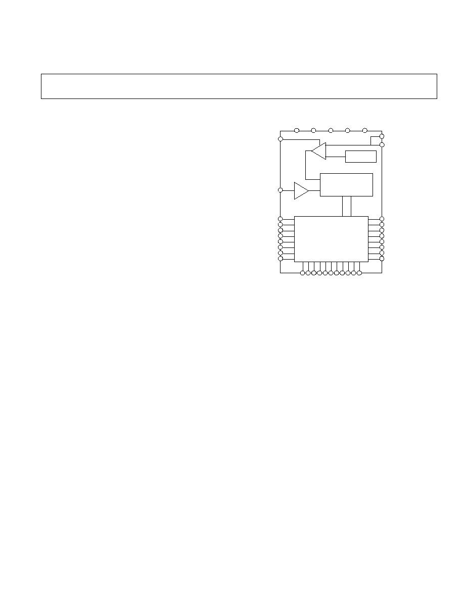
FUNCTIONAL BLOCK DIAGRAM
FEATURES
Fast Throughput Rate: 3Msps
Wide Input Bandwidth: 50MHz
No Pipeline Delays with SAR ADC
Excellent DC Accuracy Performance
Two Parallel Interface Modes
Low Power:
90mW (Full-Power) and 5mW (NAP Mode)
Standby Mode: 1µA max
Single +5V Supply Operation
Internal +2.5V Reference
Full-Scale Overrange Mode (using 15th bit)
System Offset Removal via User Access Offset Register
Nominal 0 to +2.5V Input with Shifted Range Capability
Pin Compatible Upgrade of 12-Bit AD7482
GENERAL DESCRIPTION
The AD7484 is a 14-bit, high speed, low power, succes-
sive-approximation ADC. The part features a parallel
interface with throughput rates up to 3Msps. The part
contains a low-noise, wide bandwidth track/hold amplifier
which can handle input frequencies in excess of 50MHz.
The conversion process is a proprietary algorithmic suc-
cessive-approximation technique which results in no
pipeline delays. The input signal is sampled and a conver-
sion is initiated on the falling edge of the
CONVST
signal. The conversion process is controlled via an inter-
nally trimmed oscillator. Interfacing is via standard
parallel signal lines making the part directly compatible
with microcontrollers and DSPs.
The AD7484 provides excellent ac and dc performance
specifications. Factory trimming ensures high dc accuracy
resulting in very low INL, offset and gain errors.
The part uses advanced design techniques to achieve very
low power dissipation at high throughput rates. Power
consumption in normal mode of operation is 90mW.
There are two power-saving modes: a NAP mode, which
keeps the reference circuitry alive for a quick power up
while consuming 5mW and a STANDBY mode which
reduces power consumption to a mere 5µW.
The AD7484 features an on-board +2.5V reference but
the part can also accomodate an externally-provided
+2.5V reference source. The nominal analog input range
is 0 to +2.5V but an offset shift capability allows this
nominal range to be offset by +/-200mV. This allows the
user considerable flexibility in setting the bottom end
reference point of the signal range, a useful feature when
using single-supply op-amps.
The AD7484 also provides the user with an 8% overrange
capability via a 15th bit. Thus, if the analog input range
strays outside the nominal by up to 8%, the user can still
accurately resolve the signal by using the 15th bit.
The AD7484 is powered from a +4.75V to +5.25V sup-
ply. The part also provides a V
DRIVE
pin which allows the
user to set the voltage levels for the digital interface lines.
The range for this V
DRIVE
pin is from +2.7V to +5.25V.
The part is housed in a 48-pin LQFP package and is
specified over a -40°C to +85°C temperature range.
2.5 V
REFERENCE
NAP
MODE2
BUF
T/H
AVDD AGND CBIAS DVDD DGND
VREF3
VREF1
VREF2
VIN
14-Bit Error
Correcting SAR
CS
RD
WRITE
MODE1
BUS
Y
CLIP
D0
STBY
D1
RESET
D2
VDRIVE
D3
CONVST
D4
D14
D5
D13
D6
D12
D11
D10
D9
D8
CONTROL
LOGIC AND I/O
REGISTERS
D7
AD7484

REV. PrC
7/13/01
PRELIMINARY TECHNICAL DATA
2
AD7484SPECIFICATIONS
(T
A
= 25 C, V
DD
= 4.75 V to 5.25 V, V
DRIVE
= 2.7 V to 5.25 V,
f
SAMPLE
= 3MSPS)
Parameter
Specification
Units Test Conditions/Comments
DYNAMIC PERFORMANCE
F
IN
= 100kHz Sine Wave
Signal to Noise + Distortion (SINAD)
2
78
dB min
Signal to Noise Ratio (SNR)
2
78
dB min
Total Harmonic Distortion (THD)
2
-90
dB max
Peak Harmonic or Spurious Noise (SFDR)
2
T B D
dB max
Intermodulation Distortion (IMD)
2
Second Order Terms
T B D
dB typ
Third Order Terms
T B D
dB typ
Aperture Delay
10
ns typ
Aperture Jitter
10
ps typ
Full Power Bandwidth
50
MHz typ
@ 3 dB
T B D
MHz typ
@0.1 dB
DC ACCURACY
Resolution
14
Bits
Integral Nonlinearity
2
T B D
LSB max
± 1
LSB typ
Differential Nonlinearity
2
T B D
LSB max
Guaranteed No Missed Codes to 14 bits
± 1
LSB typ
Offset Error
2
±1.5
LSB max
Gain Error
2
±1.5
LSB max
ANALOG INPUT
Input Voltage
-200
mV min
+2.7
Volts max
DC Leakage Current
T B D
µA max
Input Capacitance
10
pF typ
REFERENCE INPUT/OUTPUT
V
REF
Input Voltage
+2.5
Volts
±1% for specified performance
V
REF
Input DC Leakage Current
± 1
µA max
V
REF
Input Capacitance
T B D
pF max
V
REF
Output Voltage
+2.5
V nom
V
REF
Error @ 25°C
T B D
mV max
V
REF
Error T
MIN
to T
MAX
T B D
mV max
V
REF
Output Impedance
T B D
k typ
LOGIC INPUTS
Input High Voltage, V
INH
T B D
V min
Input Low Voltage, V
INL
0.4
V max
Input Current, I
IN
T B D
µA max
Input Capacitance, C
IN
2
T B D
pF max
LOGIC OUTPUTS
Output High Voltage, V
OH
V
DRIVE
- 0.2
V min
Output Low Voltage, V
OL
0.4
V max
Floating-State Leakage Current
T B D
µA max
Floating-State Output Capacitance
2,3
T B D
pF max
Output Coding
Straight (Natural) Binary
CONVERSION RATE
Conversion Time
T B D
ns max
Track/Hold Acquisition Time
T B D
ns max
Sine Wave Input
T B D
ns max
Full-Scale Step Input
Throughput Rate
3
MSPS max
POWER REQUIREMENTS
V
DD
+ 5
Volts
± 5 %
V
DRIVE
+2.7
V min
+5.25
V max
I
DD
Normal Mode (Static)
T B D
mA typ
Normal Mode (Operational)
18
mA typ
NAP Mode
1
mA typ
Standby Mode
1
µA max

REV. PrC
7/13/01
PRELIMINARY TECHNICAL DATA
3
AD7484
Parameter
Specification
Units Test Conditions/Comments
POWER REQUIREMENTS
(continued)
Power Dissipation
Normal Mode (Operational)
90
mW max
NAP Mode
5
mW max
Standby Mode
5
µW max
NOTES
1
Temperature ranges as follows: 40°C to +85°C.
2
See Terminology
3
Sample tested @ +25°C to ensure compliance
Specifications subject to change without notice.
TIMING CHARACTERISTICS
1,2
Parameter
Symbol
Min
Typ
Max
Units
(V
DD
= 5 V ±5%, AGND = DGND = 0 V, V
REF
= Internal;
All specifications T
MIN
to T
MAX
and valid for V
DRIVE
= 2.7 V to 5.25 V unless otherwise noted)
Data Read
Acquisition Time
t
ACQ
T B D
ns
Conversion Time
t
CONV
T B D
ns
Quiet Time before Conversion start
t
QUIET
T B D
ns
Quiet Time during Conversion
t
QUIET 2
T B D
ns
CONVST Pulse Width
t
1
T B D
ns
CONVST falling edge to BUSY falling edge
t
2
T B D
T B D
ns
CS falling edge to RD falling edge
t
3
T B D
ns
Bus Access Time
t
4
T B D
ns
CONVST falling edge to new Data valid
t
5
T B D
ns
BUSY rising edge to new Data valid
t
6
T B D
ns
Bus Relinquish Time
t
7
T B D
ns
RD rising edge to CS rising edge
t
8
T B D
ns
Data Write
WRITE Pulse Width
t
9
T B D
ns
Data Setup time
t
10
T B D
ns
Data Hold time
t
11
T B D
ns
CS falling edge to WRITE rising edge
t
12
T B D
ns
WRITE falling edge to
CS rising edge
t
13
T B D
ns
REV. PrC
7/13/01
PRELIMINARY TECHNICAL DATA
AD7484
4
CAUTION
ESD (electrostatic discharge) sensitive device. Electrostatic charges as high as 4000 V readily
accumulate on the human body and test equipment and can discharge without detection. Although
the AD7484 features proprietary ESD protection circuitry, permanent damage may occur on devices
subjected to high-energy electrostatic discharges. Therefore, proper ESD precautions are recommended
to avoid performance degradation or loss of functionality.
WARNING!
ESD SENSITIVE DEVICE
ABSOLUTE MAXIMUM RATINGS
1
(T
A
= +25°C unless otherwise noted)
V
DD
to GND . . . . . . . . . . . . . . . . . . . . . . . . . -0.3 V to +7 V
V
DRIVE
to GND . . . . . . . . . . . . . . . . . . . . . . . . -0.3 V to +7 V
Analog Input Voltage to GND . . -0.3 V to AV
DD
+ 0.3 V
Digital Input Voltage to GND . . -0.3 V to DV
DD
+ 0.3 V
REF IN to GND . . . . . . . . . . . . . -0.3 V to AV
DD
+ 0.3 V
Input Current to Any Pin Except Supplies . . . . . . . ±10mA
Operating Temperature Range
Commercial . . . . . . . . . . . . . . . . . . . . . . 40°C to +85°C
Storage Temperature Range . . . . . . . 65°C to +150°C
Junction Temperature . . . . . . . . . . . . . . . . . . . . . . . +150°C
48-Pin LQFP Package, Power Dissipation . . . . . . . . T B D
JA
Thermal Impedance . . . . . . . . . . . . . . . . . . . . 50°C/W
JC
Thermal Impedance . . . . . . . . . . . . . . . . . . . 10°C/W
Lead Temperature, Soldering
Vapor Phase (60 secs) . . . . . . . . . . . . . . . . . . . +215°C
Infared (15 secs) . . . . . . . . . . . . . . . . . . . . . . . +220°C
E S D . . . . . . . . . . . . . . . . . . . . . . . . . . . . . . . . . . . . . . . . T B D
NOTES
1
Stresses above those listed under "Absolute Maximum Ratings" may cause permanent
damage to the device. This is a stress rating only and functional operation of the device
at these or any other conditions above those listed in the operational sections of this
specification is not implied. Exposure to absolute maximum rating conditions for
extended periods may affect device reliability.
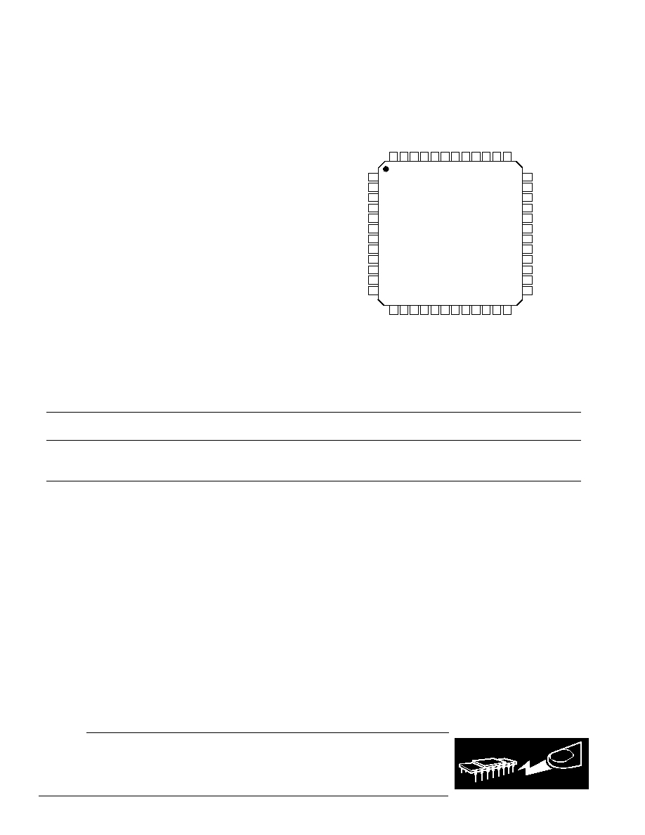
PIN CONFIGURATION
ORDERING GUIDE
Temperature
Package
Model
Range
Description
Option
AD7484BST
-40°C to +85°C
Low-profile Quad Flat Pack
ST-48
EVAL-AD7484CB
1
Evaluation Board
EVAL-CONTROL BRD2
2
Controller Board
NOTES
1
This can be used as a stand-alone evaluation board or in conjunction with the EVAL-CONTROL BOARD for evaluation/demonstration purposes.
2
This board is a complete unit allowing a PC to control and communicate with all Analog Devices evaluation boards ending in the CB designators.
AVDD
AGND
AGND
STBY
NAP
CS
RD
WRITE
BUSY
D0
D1
D2
AGND
AGND
AVDD
CLIP
MODE1
MODE2
RESET
CONVST
D14
D13
D12
D11
AVDD
CBIAS
AGND
AGND
AVDD
AGND
VIN
VREF2
VREF1
VREF3
AGND
AGND
D10
D9
D8
D7
VDRIVE
DGND
DGND
DVDD
D6
D5
D4
D3
PIN 1 IDENTIFIER
AD7484
TOP VIEW
(Not to Scale)
36
35
34
33
32
31
30
29
28
27
26
25
1
2
3
4
5
6
7
8
9
10
11
12
48
47
46
45
44
43
42
41
40
39
38
37
13
14
15
16
17
18
19
20
21
22
23
24

REV. PrC
7/13/01
PRELIMINARY TECHNICAL DATA
5
AD7484
PIN FUNCTION DESCRIPTION
Pin
Mnemonic
Description
AVDD
Positive power supply for analog circuitry.
C
BIAS
Decoupling pin for internal bias voltage. A 100nF capacitor should be placed between this pin and
AGND.
A G N D
Power supply ground for analog circuitry.
VIN
Analog input. Single-ended analog input channel.
VREF1
Reference Output. VREF1 connects to the output of the internal 2.5V reference. A 1µF capacitor must
be placed between this pin and AGND.
VREF2
Reference Input. A 1µF capacitor must be placed between this pin and AGND. When using an external
voltage reference source, the reference voltage should be applied to this pin.
VREF3
Reference decoupling pin. When using the internal reference, a 100nF must be connected from this pin
to AGND. When using an external reference source, this pin should be connected directly to AGND.
S T B Y
Standby logic input. When this pin is logic high, the device will be placed in Standby mode. See Power
Saving Section for further details.
NAP
Nap logic input. When this pin is logic high, the device will be placed in a very low power mode. See
Power Saving Section for further details.
D V D D
Positive power supply for digital circuitry.
D G N D
Ground reference for digital circuitry.
V
DRIVE
Logic Power Supply Input. The voltage supplied at this pin will determine at what voltage
the interface logic of the AD7484 will operate.
CONVST
Convert Start Logic Input. A conversion is initiated on the falling edge of
CONVST signal. The input
track/hold amplifier goes from track mode to hold mode and the conversion process commences.
RESET
Reset Logic Input. A logic 0 on this pin resets the internal state machine and terminates a conversion
that may be in progress. Holding this pin low keeps the part in a reset state.
M O D E 2
Operating Mode Logic Input. See Table 3 for details.
M O D E 1
Operating Mode Logic Input. See Table 3 for details.
CLIP
Logic input. A logic high on this pin enables output clipping. In this mode, any input voltage that is
greater than positive full scale or less than negative full scale will be clipped to all 1's or all 0's
respectively. Further details are given in the Offset / Overrange setion.
C S
Chip Select Logic Input. This pin is used in conjunction with
RD to access the conversion result. The
data bus is brought out of tri-state and the current contents of the output register driven onto the data
lines following the falling edge of both
CS and RD. CS is also used in conjunction with WRITE to
perform a write to the Offset Register.
CS can be hardwired permanently low.
R D
Read Logic Input. Used in conjunction with
CS to access the conversion result.
WRITE
Write Logic Input. Used in conjunction with
CS to write data to the Offset Register. When the desired
offset word has been placed on the data bus, the WRITE line should be pulsed high. It is the falling
edge of this pulse which latches in the word into the Offset Register.
BUSY
Busy Logic Output. This pin indicates the status of the conversion process. The
BUSY signal goes low
after the falling edge of
CONVST and stays low for the duration of the conversion. In Parallel Mode 2,
the
BUSY signal returns high when the conversion result has been clocked into the output register. In
Parallel Mode 1, the
BUSY signal returns high as soon as the conversion has been completed but the
conversion result does not get clocked into the output register until the falling edge of the next
CONVST pulse.
D0 - D13
Data I/O Bits (D13 is MSB). These are tri-state pins that are controlled by
CS, RD and WRITE.
The operating voltage level for these pins is determined by the V
DRIVE
input.
D14
Data Output Bit for overranging. If the over range feature is not used, this pin should be pulled to
DGND via a 100k resistor.

REV. PrC
7/13/01
PRELIMINARY TECHNICAL DATA
AD7484
6
TERMINOLOGY
Integral Nonlinearity
This is the maximum deviation from a straight line pass-
ing through the endpoints of the ADC transfer function.
The endpoints of the transfer function are zero scale, a
point 1/2 LSB below the first code transition, and full
scale, a point 1/2 LSB above the last code transition.
Differential Nonlinearity
This is the difference between the measured and the ideal 1
LSB change between any two adjacent codes in the ADC.
Offset Error
This is the deviation of the first code transition (00 . . .
000) to (00 . . . 001) from the ideal, i.e AGND + 0.5
L S B
Gain Error
This is the deviation of the last code transition (111 . . .
110) to (111 . . . 111) from the ideal (i.e., V
REF
1.5
LSB) after the offset error has been adjusted out.
Track/Hold Acquisition Time
Track/Hold acquisition time is the time required for the
output of the track/hold amplifier to reach its final value,
within ±1/2 LSB, after the end of conversion (the point
at which the track/hold returns to track mode).
Signal to (Noise + Distortion) Ratio
This is the measured ratio of signal to (noise + distor-
tion) at the output of the A/D converter. The signal is
the rms amplitude of the fundamental. Noise is the sum
of all nonfundamental signals up to half the sampling
frequency (f
S
/2), excluding dc. The ratio is dependent on
the number of quantization levels in the digitization
process; the more levels, the smaller the quantization
noise. The theoretical signal to (noise + distortion) ratio
for an ideal N-bit converter with a sine wave input is
given by:
Signal to (Noise + Distortion) = (6.02 N + 1.76) dB
Thus for a 14-bit converter, this is 86.04 dB.
Total Harmonic Distortion
Total harmonic distortion (THD) is the ratio of the rms
sum of harmonics to the fundamental. For the AD7484 it
is defined as:
where V
1
is the rms amplitude of the fundamental and V
2
,
V
3
, V
4
, V
5
and V
6
are the rms amplitudes of the second
through the sixth harmonics.
Peak Harmonic or Spurious Noise
Peak harmonic or spurious noise is defined as the ratio of
the rms value of the next largest component in the ADC
output spectrum (up to f
S
/2 and excluding dc) to the rms
value of the fundamental. Normally, the value of this
specification is determined by the largest harmonic in the
spectrum, but for ADCs where the harmonics are buried
in the noise floor, it will be a noise peak.
Intermodulation Distortion
With inputs consisting of sine waves at two frequencies, fa
and fb, any active device with nonlinearities will create
distortion products at sum and difference frequencies of
mfa ± nfb where m, n = 0, 1, 2, 3, etc. Intermodulation
distortion terms are those for which neither m nor n are
equal to zero. For example, the second order terms in-
clude (fa + fb) and (fa fb), while the third order terms
include (2fa + fb), (2fa fb), (fa + 2fb) and (fa 2fb).
The AD7484 is tested using the CCIF standard where two
input frequencies near the top end of the input bandwidth
are used. In this case, the second order terms are usually
distanced in frequency from the original sine waves while
the third order terms are usually at a frequency close to
the input frequencies. As a result, the second and third
order terms are specified separately. The calculation of the
intermodulation distortion is as per the THD specification
where it is the ratio of the rms sum of the individual dis-
tortion products to the rms amplitude of the sum of the
fundamentals expressed in dBs.
THD (dB )
=
20 log
V
2
2
+
V
3
2
+
V
4
2
+
V
5
2
+
V
6
2
V
1
REV. PrC
7/13/01
PRELIMINARY TECHNICAL DATA
AD7484
7
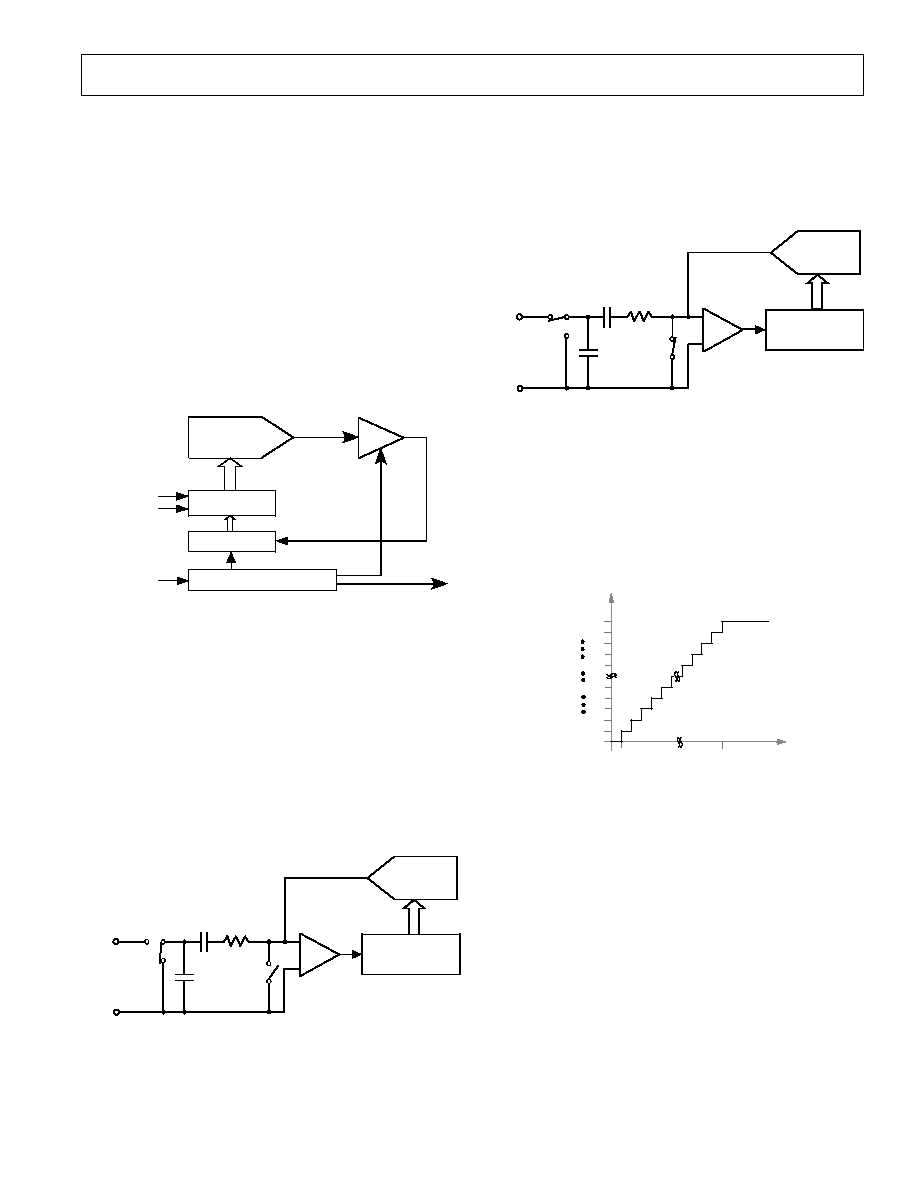
CIRCUIT DESCRIPTION
CONVERTER OPERATION
The AD7484 is a 14-bit error correcting successive ap-
proximation analog-to-digital converter based around a
capacitive DAC. It provides the user with track/hold, refer-
ence, A/D converter and versatile interface logic functions
on a single chip. The normal analog input signal range that
the AD7484 can convert is 0 to 2.5 Volts. By using the
offset and overrange features on the ADC, the AD7484 can
convert analog input signals from -200mV to +2.7V while
operating from a single +5V supply. The part requires a
+2.5V reference which can be provided from the part's own
internal reference or an external reference source. Figure 1
shows a very simplified schematic of the ADC. The Control
Logic, SAR and the Capacitive DAC are used to add and
subtract fixed amounts of charge from the sampling capaci-
tor to bring the comparator back to a balanced condition.
Figure 1. Simplified Block Diagram of AD7484
CAPACITIVE
DAC
COMPARATOR
CONTROL LOGIC
+
-
SW1
SW2
AGND
VIN
A
B
CAPACITIVE
DAC
COMPARATOR
CONTROL LOGIC
+
-
SW1
SW2
AGND
VIN
A
B
Figure 2. ADC Conversion Phase
Figure 3. ADC Acquisition Phase
At the end of conversion, the track/hold returns to track-
ing mode and the acquisition time begins. The track/hold
acquisition time is TBD nS. Figure 3 shows the ADC
during its acquistition phase. SW2 is closed and SW1 is
in position A. The comparator is held in a balanced con-
dition and the sampling capacitor acquires the signal on
V
IN
.
Conversion is initiated on the AD7484 by pulsing the
CONVST input. On the falling edge of CONVST, the
track/hold goes from track to hold mode and the conversion
sequence is started. Conversion time for the part is TBD
nS. Figure 2 shows the ADC during conversion. When
conversion starts, SW2 will open and SW1 will move to
position B causing the comparator to become unbalanced.
The ADC then runs through its successive approximation
routine and brings the comparator back into a balanced
condition. When the comparator is rebalanced, the conver-
sion result is available in the SAR register.
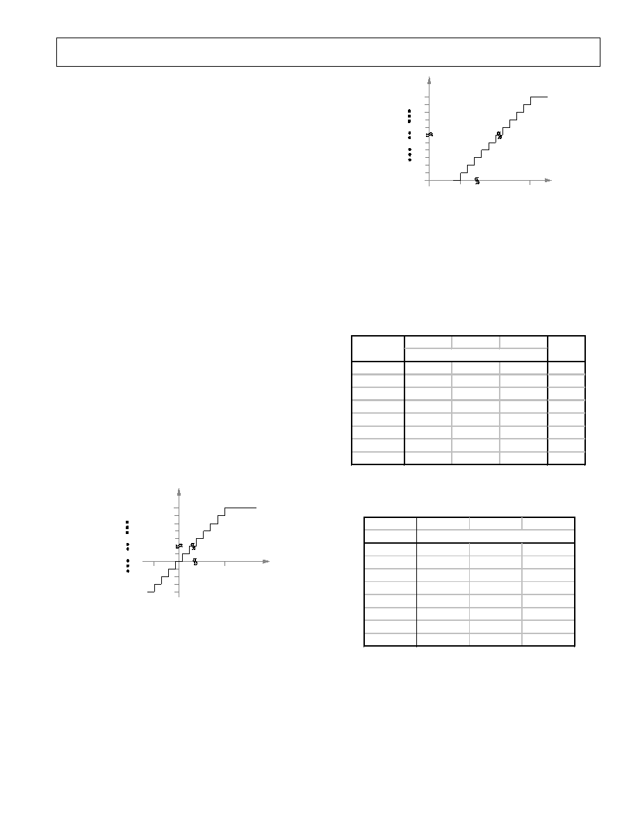
ADC TRANSFER FUNCTION
The output coding of the AD7484 is straight binary. The
designed code transitions occur midway between successive
integer LSB values (i.e., 1/2 LSB, 3/2 LSBs, etc.). The
LSB size is V
REF
/ 16384. The nominal transfer characteris-
tic for the AD7484 in shown in figure 4 below. This
transfer characteristic may be shifted as detailed in the Off-
set/Overrange section.
000...000
0V
A
D
C
C
O
D
E
ANALOG INPUT
111...111
000...001
000...010
111...110
111...000
011...111
0.5LSB
+VREF-1.5LSB
1LSB = VREF/16384
Figure 4. AD7484 Transfer Characteristic
SAR
14-BIT PARALLEL
CAPACITIVE
DAC
COMPARATOR
OUTPUT DATA
CONTROL LOGIC
CONTROL
INPUTS
SWITCHES
VIN
VREF
REV. PrC
7/13/01
PRELIMINARY TECHNICAL DATA
AD7484
8
20
25
30
35
40
45
50
55
60
0
500
1000
1500
2000
2500
3000
THROUGHPUT - KSPS
POWER - mW
1 µS
300 nS
700 nS
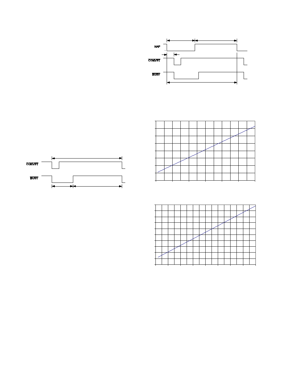
POWER SAVING
The AD7484 uses advanced design techniques to achieve
very low power dissipation at high throughput rates. In addi-
tion to this the AD7484 features two power saving modes,
Nap Mode and Standby Mode. These modes are selected by
bringing either the NAP or STBY pin to a logic high respec-
tively.
When operating the AD7484 in normal, fully powered
mode, the current consumption is 18mA during conver-
sion and the quiescent current is 5mA. Operating at a
throughput rate of 1MSPS, the conversion time of 300nS
contributes 27mW to the overall power dissipation.
Figure 5. Normal Mode Power Dissipation
Figure 6. NAP Mode Power Dissipation
(400nS / 1µS) x (5V x 18mA) = 36mW
While in NAP mode for the rest of the cycle, the AD7484
dissipates only 3mW of power.
(600nS / 1µS) x (5V x 1mA) = 3mW
Figure 5 below shows the AD7484 conversion sequence
operating in normal mode.
In NAP mode, all the internal circuitry except for the
internal reference is powered down. In this mode, the
power dissipation of the AD7484 is reduced to 5mW.
When exiting NAP mode a minimum of 100nS must be
waited before initiating a conversion. This is necessary to
allow the internal circuitry to settle after power-up and for
the track/hold to properly acquire the analog input signal.
If the AD7484 is put into NAP mode after each conversion,
the average power dissipation will be reduced but the
throughput rate will be limited by the power-up time. Using
the AD7484 with a throughput rate of 1MSPS while placing
the part in NAP mode after each conversion would result in
average power dissipation as follows: The power-up and
conversion phase will contribute 36mW to the overall power
dissipation.
(300nS / 1µS) x (5V x 18mA) = 27mW
For the remaining 700nS of the cycle, the AD7484 dissipates
17.5mW of power.
(700nS / 1µS) x (5V x 5mA) = 17.5mW
Thus the power dissipated during each cycle is:
27mW + 17.5mW = 44.5mW
Thus the power dissipated during each cycle is:
36mW + 3mW = 39mW
Figure 6 shows the AD7484 conversion sequence if putting
the part into NAP mode after each conversion.
400nS
1 µS
600nS
100nS
Figures 7 and 8 show a typical graphical representation of
Power vs. Throughput for the AD7484 when in Normal and
Nap modes respectively.
0
5
10
15
20
25
30
35
40
45
50
0
250
500
750
1000
1250
1500
1750
2000
THROUGHPUT - KSPS
POWER - mW
Figure 7. Normal Mode - Power vs. Throughput
Figure 8. Nap Mode - Power vs. Throughput
In STANDBY mode, all the internal circuitry is powered
down and the power consumption of the AD7484 is re-
duced to 5µW. The power-up time necessary before a
conversion can be initiated is longer because the internal
reference has been powered down. If using the internal
reference of the AD7484, the ADC must be brought out
of STANDBY mode 200µS before a conversion is initi-
ated. Initiating a conversion before the required power-up
time has elapsed will result in incorrect conversion data.
If an external reference source is used and kept powered
up while the AD7484 is in STANDBY mode, the power-
up time required will be reduced.
REV. PrC
7/13/01
PRELIMINARY TECHNICAL DATA
AD7484
9
OFFSET / OVERRANGE
The AD7484 provides a ±8% overrange capability as well as
a programmable Offset Register. The overrange capability is
achieved by the use of a 15th bit (D14) and the CLIP input.
If the CLIP input is at logic high and the contents of the
offset register are zero, then the AD7484 operates as a nor-
mal 14-bit ADC. If the input voltage is greater than the
full-scale voltage, the data output from the ADC will be all
1's. Similarly, if the input voltage is lower than the zero-
scale voltage, the data output from the ADC will be all 0's.
In this case D14 acts as an overrange indicator. It is set to a
1 if the analog input voltage is outside the nominal 0 to
+2.5V range.
If the Offset Register contains any value other than zero,
the contents of the register are added to the SAR result at
the end of conversion. This has the effect of shifting the
transfer function of the ADC as shown in Figure 9 and Fig-
ure 10. However, it should be noted that with the CLIP
input set to logic high, the maximum and minimum codes
that the AD7484 will ouput will be 0x3FFF and 0x0000
respectively. Further details are given in Table 1 and Table
2.
Figure 9 shows the effect of writing a positive value to the
Offset Register. If, for example, the contents of the Offset
Register contained the value 1024, then the value of the ana-
log input voltage for which the ADC would transition from
reading all 0's to 000...001 (the bottom reference point)
would be:
0.5LSB - (1024 LSBs) = -156.326mV
The analog input voltage for which the ADC would read
full-scale (0x3FFF) in this example would be:
2.5V -1.5LSBs - (1024 LSBs) = 2.34352V
000...000
0V
A
D
C
C
O
D
E
ANALOG INPUT
111...111
000...001
000...010
111...110
111...000
011...111
+VREF-1.5LSB
-OFFSET
1LSB = VREF/16384
0
.
5
L
S
B
-
O
F
F
S
E
T
Figure 9. Transfer Characteristic With Positive Offset
The effect of writing a negative value to the Offset Register is
shown in Figure 10. If a value of -512 was written to the
Offset Register, the bottom end reference point would now
occur at:
0.5LSB - (-512 LSBs)= +78.20mV
Following from this, the analog input voltage needed to
produce a full-scale (0x3FFF) result from the ADC would
now be:
2.5V - 1.5LSBs - (-512 LSBs) = 2.5779V
000...000
0V
A
D
C
C
O
D
E
ANALOG INPUT
111...111
000...001
000...010
111...110
111...000
011...111
0.5LSB
-OFFSET
+VREF-1.5LSB
-OFFSET
1LSB = VREF/16384
Figure 10. Transfer Characteristic With NegativeOffset
Table 1 below shows the expected ADC result for a given
analog input voltage with different offset values and with
CLIP tied to logic high. The combined advantages of the
offset and overrange features of the AD7484 are shown
clearly in Table 2. It shows the same range of analog in-
put and offset values as Table 1 but with the clipping
feature disabled.
Values from -1310 to +1310 may be written to the Offset
Register. These values correspond to an offset of ±200mV. A
write to the Offset Register is performed by writing a 15-bit
word to the part as detailed in the Interfacing sections. The
12 LSBs of the 15-bit word contain the offset value, the 3
MSBs must be set to zero. Failure to write zeros to the 3
MSBs may result in the incorrect operation of the device.
Table 1. Clipping Enabled (CLIP = 1)
OFFSET
-512
0
+1024
VIN
ADC DATA, D[0:14]
-200m V
-1822
-1310
-286
-156.3m V
-1536
-1024
0
0V
-512
0
1024
+78.2m V
0
512
1536
+2.3435V
14847
15359
16383
+2.5V
15871
16383
17407
+2.5779V
16383
16895
17919
+2.7V
17182
17694
18718
Table 2. Clipping Disabled (CLIP = 0)
OFFSET
-512
0
+1024
VIN
ADC DATA, D[0:13]
D14
-200mV
0
0
0
1
-156.3mV
0
0
0
1
0V
0
0
1024
0
+78.2mV
0
512
1536
0
+2.3435V
14847
15359
16383
0
+2.5V
15871
16383
16383
0
+2.5779V
16383
16383
16383
1
+2.7V
16383
16383
16383
1
REV. PrC
7/13/01
PRELIMINARY TECHNICAL DATA
7/13/01 5 PM
AD7484
1 0
Figure 11. AD7484 Typical Connection Diagram
PARALLEL INTERFACE
The AD7484 features two parallel interfacing modes.
These modes are selected by the Mode pins as detailed in
Table 3.
2
e
d
o
M
1
e
d
o
M
d
e
s
U
t
o
N
0
0
1
e
d
o
M
l
e
l
l
a
r
a
P
0
1
2
e
d
o
M
l
e
l
l
a
r
a
P
1
0
d
e
s
U
t
o
N
1
1
Table 3. AD7484 Operating Modes
In Parallel Mode 1, the data in the output register is up-
dated and available for reading when
BUSY returns high
at the end of a conversion. This mode should be used if
the conversion data is required immediately after the con-
version has completed. An example where this may be of
use is if the AD7484 were operating at much lower
throughput rates in conjunction with Nap Mode (for
power-saving reasons) and the input signal being com-
pared with set limits. If the limits were exceeded, the
ADC would then be woken up and commence sampling at
full speed. Figure 12 shows a timing diagram for the
AD7484 operating in Parallel Mode 1.
In Parallel Mode 2, the data in the output register is not
updated until the next falling edge of
CONVST. This
mode could be used where a single sample delay is not
vital to the system operation. This may occur, for ex-
ample, in a system where a large amount of samples are
taken at high speed before a Fast Fourier Transform is
performed for frequency analysis of the input signal. Fig-
ure 13 shows a timing diagram for the AD7484 operating
in Parallel Mode 2.
Reading Data from the AD7484
Data is read from the part via a 15-bit parallel data bus
with the standard
CS and RD signals. The CS and RD
signals are internally gated to enable the conversion result
onto the data bus. The data lines D0 to D14 leave their
high impedance state when both
CS and RD are logic low.
Therefore,
CS may be permanently tied logic low if re-
quired and the
RD signal used to access the conversion
result. Figures 12 and 13 show timing specifications
called t
QUIET
and t
QUIET2
. The quiet time, t
QUIET
, is the
amount of time that should be left after any data bus activ-
ity before the next conversion is initiated. The second
quiet time, t
QUIET2
, is the period during a conversion where
activity on the data bus should be avoided. Reading a re-
sult from the AD7484 while the latter half of the
conversion is in progress will result in the degradation of
performance by about TBD dB.
Writing to the AD7484
The AD7484 features a user accessible offset register.
This allows the bottom of the transfer function to be
shifted by ±200mV. This feature is explained in more
detail in the Offset / Overrange section.
To write to the offset register a 15-bit word is written to
the AD7484 with the 12 LSBs containing the offset value
in 2's complement format. The 3 MSBs must be set to
zero. The offset value must be within the range -1310 to
+1310, corresponding to an offset from -200mV to
+200mV. The value written to the offset register is stored
and used until power is removed from the device. The
value stored may be updated at any time between conver-
sions by another write to the device. Table 4 shows some
examples of offset register values and their effective offset
voltage. Figure 14 shows a timing diagram for writing to
the AD7484.
Typical Connection
Figure 11 shows a typical connection diagram for the
AD7484 operating in Parallel Mode 1. Conversion is
initiated by a falling edge on
CONVST. Once CONVST
goes low, the
BUSY signal goes low and at the end of
conversion, the rising edge of
BUSY is used to activate an
Interrupt Service Routine. The
CS and RD lines are then
activated to read the 14 data bits (15 bits if using the
overrange feature).
In Figure 11 the V
DRIVE
pin is tied to DV
DD
, which results
in logic output levels being either 0 V or DV
DD
. The volt-
age applied to V
DRIVE
controls the voltage value of the
output logic signals. For example, if DV
DD
is supplied by
a 5 V supply and V
DRIVE
by a 3 V supply, the logic output
levels would be either 0 V or 3 V. This feature allows the
AD7484 to interface to 3 V devices while still enabling the
ADC to process signals at 5 V supply.
Table 4. Offset Register Examples
Code (De c) D14-D12 D11-D0 (2's Comp) Offset (mV)
-1310
000
101011100010
-200
-512
000
111000000000
-78.12
+256
000
000100000000
+39.06
+1310
000
010100011110
+200
AD7484
AV
DD
1nF
ANALOG
SUPPLY
4.75V - 5.25V
REF1
µ
C/
µ
P
VIN
0V to
+2.5V
0.47µF
PARALLEL
INTERFACE
D0-D14
CS
CONVST
RD
BUSY
V
DRIVE
DV
DD
10µF
47µF
0.1µF
0.47µF
REF2
REF3
0.1µF
STBY
NAP
CLIP
WRITE
MODE2
MODE1
RESET
0.1µF
V
BIAS
REV. PrC
7/13/01
PRELIMINARY TECHNICAL DATA
AD7484
1 1
t1
t2
t
ACQ
t5
t3
t
QUIET
Data N
Data N+1
t4
t
QUIET 2
t
CONV
t1
t2
t4
t6
t3
t7
t8
t
QUIET 2
t
QUIET
t
ACQ
t
CONV
t9
t10
t11
t12
t13
Figure 12. Parallel Mode 1 Read Cycle
Figure 13. Parallel Mode 2 Read Cycle
Figure 14. Parallel Mode Write Cycle
REV. PrC
7/13/01
PRELIMINARY TECHNICAL DATA
1 2
AD7484
OUTLINE DIMENSIONS
Dimensions shown in inches and (mm).
48-Pin LQFP Package (ST-48)
TOP VIEW
(PINS DOWN)
1
12
13
25
24
3 6
37
4 8
0.019 (0.5)
BSC
0.276
(7.00)
BSC
SQ
0.011 (0.27)
0.006 (0.17)
0.354 (9.00) BSC SQ
0.063 (1.60)
MAX
0.030 (0.75)
0.018 (0.45)
0.008 (0.2)
0.004 (0.09)
0
MIN
COPL ANARITY
0.003 (0.08)
SEATING
PL ANE
0.006 (0.15)
0.002 (0.05)
7
0
0.057 ( 1.45)
0.053 ( 1.35)
Document Outline
- Specifications
- Pinout
- Package Drawings
- Ordering Guide
- Features
- Product Description
- Timing characteristics
- Absolute Maximum Ratings
- Functional Block Diagram
- Circuit Description
- OPERATION
- ADC TRANSFER FUNCTION
- POWER SAVING
- OFFSET / OVERRANGE
- PARALLEL INTERFACE
- DIAGRAMS
- Parallel Mode Write Cycle
- Parallel Mode 2 Read Cycle
- Parallel Mode 1 Read Cycle
- AD7484 Typical Connection Diagram
- Normal Mode Power Dissipation
- NAP Mode Power Dissipation
- AD7484 Transfer Characteristic
- ADC Acquisition Phase
- ADC Conversion Phase
- Simplified Block Diagram of AD7484